Заглавная страница Избранные статьи Случайная статья Познавательные статьи Новые добавления Обратная связь FAQ Написать работу КАТЕГОРИИ: ТОП 10 на сайте Приготовление дезинфицирующих растворов различной концентрацииТехника нижней прямой подачи мяча. Франко-прусская война (причины и последствия) Организация работы процедурного кабинета Смысловое и механическое запоминание, их место и роль в усвоении знаний Коммуникативные барьеры и пути их преодоления Обработка изделий медицинского назначения многократного применения Образцы текста публицистического стиля Четыре типа изменения баланса Задачи с ответами для Всероссийской олимпиады по праву 
Мы поможем в написании ваших работ! ЗНАЕТЕ ЛИ ВЫ?
Влияние общества на человека
Приготовление дезинфицирующих растворов различной концентрации Практические работы по географии для 6 класса Организация работы процедурного кабинета Изменения в неживой природе осенью Уборка процедурного кабинета Сольфеджио. Все правила по сольфеджио Балочные системы. Определение реакций опор и моментов защемления |
Studying of light-emitting diodeСодержание книги
Поиск на нашем сайте
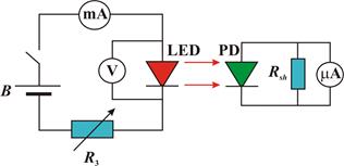
2) Goal: Studying of electric energy transformation into light one by the LED and measuring its electric and light characteristics. 3) Scheme of laboratory research facility:
4) Table of measuring instruments:
Accesories: the LED, the photodiode. 5) Equations for calculation: 1. Electrical power consumed by LED:
where I 1 (LED) – current through LED, U – forward bias voltage. 2. Light emission power:
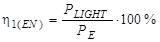
where I 2 (PD) – current through photodiode, S – photodiode sensitivity. 3. LED energy efficiency:
where PLIGHT - light emission power, PE - electrical power consumed by LED. 4. LED quantum efficiency:
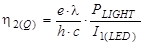
where e = 1.6·10-19 - charge of electron, λ - wavelength of light, h =6.63·10-34J·s - Planck constant, c = 3·108 m/s - speed of light, PLIGHT - light emission power, I 1 (LED) – current through LED. 6) Table of measurements S = … μA/mW - the photodiode sensitivity (imprinted on the box), λ = … nm, Rsh = 1 kΩ (grid limit 500 μА); Rsh = 500 Ω (Grid limit 1000 μА).
7) Quantities calculation: UCUT = … V; RRES = … Ω; 8) Graph:
9) Final results: UCUT = … V; RRES = … Ω; η 1 (EN) (50mA) = …%; η 2 (Q) (50mA) = …%. 10) Conclusions: 11) Work done by:Work checked by:
LABORATORY WORK № 6 – 10 Topic: STUDYING OF A PHOTOELECTRIC EFFECT IN A P-N JUNCTION Goal of the work Studying the photoelectric effect in a p-n junction and measuring of dark and light current-voltage characteristics. Main concepts 3.1 P-N junction ( see work 6-9 ) Photodiode properties
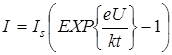
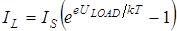
Photovoltaic effect consists in appearing of a photo-emf in a valve (i.e. rectifying) contact while it’s illuminated. The lowest frequency f0 (the highest wavelength λ 0 ) at which the photoelectric effect still possible called the photoelectric effect red border. It can be determined for given semiconductor from the condition: hf0 = Eg, that means that energy of photons hf0 must be not less than the forbidden energy gap width. On the Fig. 19 (curve 1) represented current-voltage characteristic of non-illuminated p-n junction. It can be described by such equation:
here IS – saturation current of non-illuminated p-n junction, k – Boltzman constant, e – elementary charge, T – temperature in Kelvins, U – external applied voltage.
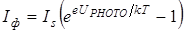
Now let’s p-n junction be illuminated by light with energy of photons not less then forbidden gap width of the semiconductor. The internal photoelectric effect will lead to generation of electron-hole pairs, concentration of which will decrease with increasing of distance from illuminated surface. Electrons and holes will move to the junction, where they will be separated. Majority carriers of the region will be held by internal built-in electric field. Accelerated minority carriers will freely path through p-n junction, and create photocurrent IPHOTO, which flows in the reverse direction (from n- to p - region). If the circuit is open, then on the borders of p-n junction appears volume charge that opposes to further migration of charge carriers. This volume charge produces photo-emf U0 with polarity reverse to polarity of built-in potential. Potential barrier of depletion region decreases (Fig. 18b). That leads to appearance of leakage current IL flowing in the reverse direction. The photo-emf will be increased until the photocurrent will be compensated by increasing current of majority carriers. If we connect to p-n junction load resistance RLOAD (Fig. 20), than, in obtained circuit will flow a current I which can be represented as: I = IPHOTO - IL (47) Leakage current IL can be calculated by formula (46) for non-illuminated p-n junction when an external forward bias voltage ULOAD = I×RLOAD is applied:
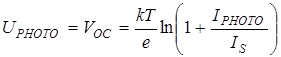
Let’s consider the critical modes of operation of such photocell. 1.Short-circuit mode appears if RLOAD = 0. Then ULOAD = 0, IL = 0 and short circuit current ISC is equal to photocurrent IPHOTO which is proportional to light intensity Ф: ISC = IPHOTO; IPHOTO ~ Ф (48) 2.Open-circuit mode will take place if RLOAD = ¥. The open-circuit voltage VOC = UPHOTO, total current I = 0 and IPHOTO = IL. Equation (46) gives
from where we get
where UPHOTO – is a photo EMF generated in the photocell.
Thus, valve photocells allow to transform radiant energy directly into electric one. That is why they also called the photogalvanic elements and used as sources of EMF in the solar cell batteries. The current-voltage characteristic of illuminated p-n junction shown on the Fig.19 (curve2). Segment OA (U = 0) refers to short-circuit current (RLOAD = 0), segment OB (I = 0) – to open-circuit voltage (RLOAD =∞). Changing external load from 0 to ∞ we’ll get segment AB, which is a current-voltage characteristic of p-n junction in a photogalvanic mode at constant light intensity Ф. Segment BC characterize work of the photocell at forward bias voltage, segment AD – at reverse bias (photodiode mode). The CVCs will be displaced and change their shape under the change of light flux intensity. The photocell CVCs in a photogalvanic mode for different light intensities are shown on the figure 21. Straight line, drawn from the coordinate origin under the angle α (
Optimal load resistance
where Ф – light intensity in Watts, P – useful power, emitted on the load. 4 Data processing (Same as in lab № 8.5)
|
|||||||||||||||||||||||||||||||||||||||||||||||||||||||||||||||||||||||||||||||||||||||||||||||||||||||||||||||||||||||||||||||||||||||||||||
|
|
Последнее изменение этой страницы: 2016-04-26; просмотров: 275; Нарушение авторского права страницы; Мы поможем в написании вашей работы! infopedia.su Все материалы представленные на сайте исключительно с целью ознакомления читателями и не преследуют коммерческих целей или нарушение авторских прав. Обратная связь - 18.119.127.230 (0.006 с.) |

 ;
; ;
; ;
; .
.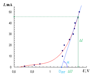
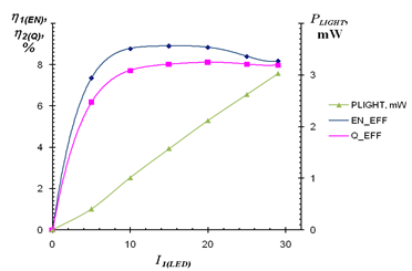
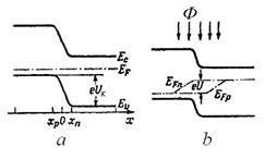 Figure 18 – Band diagram of non-illuminated (а) and illuminated (b) p-n junction.
 (46)
(46)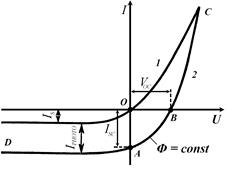 Figure 19 – CVC of the non-illuminated (curve 1) and illuminated (curve 2) р-n-junction.
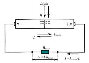 Figure 20 – Principle of operation of the photocell.
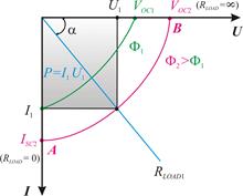 Figure 21 – photocells’ CVC at different light intensities.
 .
. (49)
(49) (50)
(50)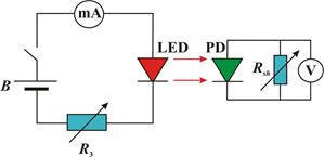 Figure 22 – Scheme of work 6-10 research facility
 ), intersects the CVC at point, which X coordinate is equal to voltage drop on the load RLOAD, and Y coordinate – current in the external circuit (for example U 1 = I 1· RLOAD 1). Highlighted area (Fig.21) is proportional to power P, generated on the load RLOAD 1:
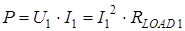 (51)
(51) chosen in such way that this power will be maximal. Efficiency of the photogalvanic cell η determined as:
 (52)
(52)