Заглавная страница Избранные статьи Случайная статья Познавательные статьи Новые добавления Обратная связь FAQ Написать работу КАТЕГОРИИ: ТОП 10 на сайте Приготовление дезинфицирующих растворов различной концентрацииТехника нижней прямой подачи мяча. Франко-прусская война (причины и последствия) Организация работы процедурного кабинета Смысловое и механическое запоминание, их место и роль в усвоении знаний Коммуникативные барьеры и пути их преодоления Обработка изделий медицинского назначения многократного применения Образцы текста публицистического стиля Четыре типа изменения баланса Задачи с ответами для Всероссийской олимпиады по праву 
Мы поможем в написании ваших работ! ЗНАЕТЕ ЛИ ВЫ?
Влияние общества на человека
Приготовление дезинфицирующих растворов различной концентрации Практические работы по географии для 6 класса Организация работы процедурного кабинета Изменения в неживой природе осенью Уборка процедурного кабинета Сольфеджио. Все правила по сольфеджио Балочные системы. Определение реакций опор и моментов защемления |
State service of communicationСодержание книги
Поиск на нашем сайте ODESSA NATIONAL ACADEMY OF TELECOMMUNICATIONS After A. S. POPOV ====================================================================== Department of physics of optical communications
PHYSICS of OPTICAL COMMUNICATION Module 2.3: Physics of optical communication PART 3: LABORATORY WORKS for bachelor training of educational area 0924 –“Telecommunications”
APPROVED by the Faculty Council Protocol № 4 from 19.11.2010 ODESSA 2012 UDK 538 (075.8) Publication plan 2012.
Writers: assoc. prof. Gorbachov V.E, instructor Kardashev K.D.
The following methodical guide is about section “Optics” of physics course for telecommunications technician. Six laboratory works allow students to learn basics of geometrical optics, wave optics and polarization phenomenon including birefringence. It contains sufficient theoretical information combined with detailed descriptions of applied equipment construction and measuring techniques for exploring properties of light. Recommended for students of TE-group, educational area 0924 –“Telecommunications”.
CONFIRMED at the Department session Protocol № 4 from 26.11.2010 INTRODUCTION The main goal of this laboratory course is advancing of theoretical knowledge on processes in devices of optical communication and familiarization of students with methods of investigation and measurement of different parameters of systems of optical communication. This laboratory works are made on a base of light emitted diode and photodiode. All laboratory works are provided in a frontal way, i.e. all group makes the same laboratory work at the same time. Appropriate homework must forego to work in a lab. The homework contains self-studying of theory and methodology of work accomplishment, preparation of protocol which includes experimental facility’s schematic drawing, equipment table's drawing, measurement table's drawing, a list of working formulae with description of all quantities which are in, list of test questions' answering. The allowance to performing of laboratory work will be had only those of students who have fulfilled homework and have positive result on express mini-quiz in a lab.
Content of the reports for all laboratory works has to be the following: 1) Number and title of laboratory work. 2) Goal of the work. 3) Laboratory-research facility's scheme. 4) Equipment table. 5) Equations for calculation with decryption of all quantities in. 6) Standard table of measurements for each measured quantity. It has to be checked and verified by an instructor. 7) Experimental data processing. 8) Standard form of result (confidence interval and relative error or a graphic result) 9) Conclusion 10) Date, name of a student. Besides this guide is recommended to use literature from bibliography given at the end of this guide. LIST OF LABORATORY WORKS
LABORATORY WORK № 8-5 1 Topic:STUDYING PHOTOCONDUCTIVITY OF HOMOGENEOUS SEMICONDUCTORS 2 Goal of the work: 1.1. Learning basic of internal photoelectric effect theory. 1.2. Acquaintance with the method of investigation of photoelectric properties of semiconductor. 1.3. Measurement of the lux-ampere characteristic in order to elucidate recombination mechanism of nonequilibrium charge carriers. Main concepts Photoconductivity is a phenomenon of change of electrical conductivity of crystals at light exposing due to the internal photoelectric effect. The internal photoelectric effect is a process of generation of charge carriers under the action of light, leading to increase of electrical conductivity.
The intrinsic photoconductivity is conductivity caused by light-induced transition of electrons from the valence band to the conductivity band. In this case, obviously, that the photon energy hν should satisfy the condition hν ³ Е g. Consequently, there is some boundary minimal frequency ν RB, at which the photoconductivity still observed. It is determined by the ratio hν RB= Е g. Corresponding boundary maximal wavelength λRB= c / ν RB called photoelectric threshold or red (long-wavelength) border of photoeffect. For example, for a semiconductor with a band gap Е g=2 eV we obtain boundary frequency ν RB= Е g / h =5ּ1014 s – 1, which corresponds to a long-wavelength border λRB=0,6ּ10 – 6 m. The impurity photoconductivity that appears during light-induced transitions types 2 and 3 (see Fig. 1) has a small probability, because at room temperature all impurity levels are already ionized. Detailed studying of the internal photoelectric effect shows that concentration of photocarriers at given intensity of light flux depends on its chemical composition. That is why each semiconductor has its own spectral characteristics (range of photosensitivity). In darkness semiconductor has any concentration of equilibrium electrons n 0 and holes р 0. During a light exposure the generation of excess (nonequilibrium) electron-hole pairs leads to increase in electrical conductivity of the semiconductor. Total conductivity, in the presence of nonequilibrium electrons Δ n and holes Δ р, can be written as:
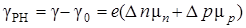
Photoconductivity – is the excess conductivity, equal to the difference of conductivities of semiconductor at presence of illumination γ and in its absence γ0:
At continuous illumination by a white light (with equal intensity for all wavelengths), the steady-state concentration of nonequilibrium carriers Δ n and Δ р depend from the intensity of light.
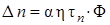
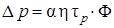
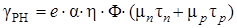
where τ n и τ р – lifetime of electrons and holes respectively (time over which the carrier concentration decreases in e times after switching-off of illumination); h – quantum efficiency (number of electron-hole pairs, generated by one absorbed photon); α – absorption coefficient. In (3) quantum intensity of light Φ is equal an amount of photons, which fall on 1 m 2 of surface per 1 s. Then common light intensity I =Φ× hν, where hν – energy of one photon. From (2) and (3) we obtain dependence of stationary photoconductivity from light intensity, during continuous illumination:
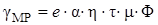
If one of the terms in parentheses of equation (4) is significantly larger than the other (due to the difference in values of mobility or the lifetime of electron and hole), then, the photoconductivity is determined by the carriers of one sign, and called monopolar. In this case
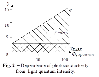
Value τdetermined by conditions of recombination of charge carriers in the semiconductor and depends on many factors. In the simplest case it is a constant. Investigating the dependance of γPH from light intensity I (measuring the lux-ampere characteristics of the semiconductor) we can get some information about the conditions of recombination of charge carriers in a semiconductor. When semiconductor is illuminated with monochromatic light, it can be considered, that α=const and h=const. Linear dependence γPH from quantum intensity of light Φmeans, that the lifetime τ=const, i.e. it does not depend on the concentration of nonequilibrium carriers of charge. This is co-called linear recombination. If the dependence γPH from Φsublinear, i.e. γPH~ Ιа, where а <1, it means, that τ decreases with increasing light intensity, or, that is the and same, with increasing concentration of nonequilibrium carriers of charge. It is observed at high intensities of illumination.
On a Fig. 2 represented plot of photoconductivity versus quantum intensity of light Φ. The phenomenon of photoconductivity in semiconductors is widely used for measuring parameters of semiconductor materials, as well as in engineering to create a light-sensitive devices - photoresistors.
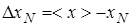
Data processing For representation of the result of direct measurements of quantity x: 1) Obtain the sequence of measured values x 1, x 2, x 3, ..., xN and write result of these n measurements in a second column of Table of measurements. In a first column of Table of measurements write an ordinal number of measurement. 2) Calculate the average value of measurand:
3) Find an abmodality of each measurement and write result in a third column of Table of measurements:
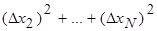
4) Square each abmodality in a fourth column of Table of measurements and summarize them:
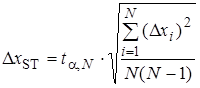
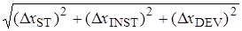
5) Find a statistical absolute error D x ST of measurements from Student’s equation:
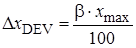
where a – confidence probability; N – total number of measurements; t a; N – Student’s coefficient. 6) If it is not identified an absolute instrumental error D x INST on measuring tool, it is necessary to find a device absolute error of measurements from accuracy class b of electrical measuring instrument:
where х max – grid limit. 7) Find a total absolute error of measurements
8) Calculate relative error of measurements:
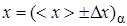
9) Final result of direct measurements should be represented by a confidence interval and relative error:
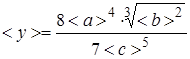
For representation of the result of indirect measuring of quantity y it is necessary: 1) Calculate the average value of measurand < y > by formula from average values of known quantities < a >, < b >, < c >, for example:
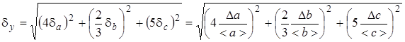
2) Calculate relative error of measurand d y from relative errors of known quantities d a, d b, d c by formula that should be gained accordingly to this example:
where D a, D b, D c – absolute errors of known quantities; < a >, < b >, < c > – its average values. 3) Find an absolute error of measurand
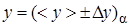
4) Final result of indirect measuring should be represented by a confidence interval and relative error:
5 Description of laboratory research facility and methodology of measurements The experimental laboratory-research facility consists of semiconductor sample connected to a digital multimeter (set as Ohm-meter) and illuminator (see scheme in the protocol below). The sample is situated in front of the illuminator. Intensity of illumination of the sample is changed by changing the distance between sample and the illuminator lamp.
|
||||||||||||||||||||||||||||||||||||||||||||||||||||
|
|
Последнее изменение этой страницы: 2016-04-26; просмотров: 291; Нарушение авторского права страницы; Мы поможем в написании вашей работы! infopedia.su Все материалы представленные на сайте исключительно с целью ознакомления читателями и не преследуют коммерческих целей или нарушение авторских прав. Обратная связь - 216.73.216.214 (0.009 с.) |


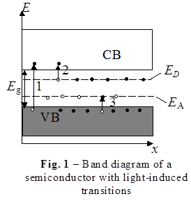 The primary process for the internal photoelectric effect is absorption of a photon with energy, sufficient for the transition of electron from valence band and donor level to conductivity band, as well as from valence band to acceptor level. On a Fig. 1 represented possible types of transitions, leading to changes in electrical conductivity. Transition 1 leads to generation of electron-hole pair, transitions 2 and 3 produce charge carriers of one sign from impurity atom (only electrons from donor impurity for transition 2, and only holes from acceptor impurity for 3).
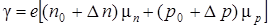
 ;
; ,
,
 Under certain conditions, dependence γPH from Φ can be superlinear. This means, that τ increases with increasing of light intensity, due to the complex processes of recharging of trapping centres in the semiconductor, leading to significant changes in the conditions of recombination of charge carriers.
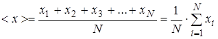 .
.
 ;
;  ;...;
;...;  .
.


 .
.
 ,
,
 ,
,
 .
.
 .
.
 = (… ± …)0.95;
 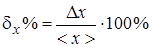 = … %.
 .
.
 ,
,
 = (… ± …)0.95;
 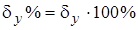 = … %
= … %